Balancing speed with quality and adherence to strict schedules while maintaining circuit board cost-effectiveness.
Handling intricate designs with multiple high-speed signals, mixed-signal components, and tight tolerances, especially when integrating FPGAs.
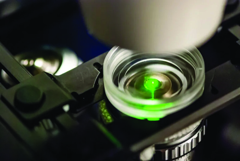
Maintaining signal quality and minimizing noise and interference, is crucial for high-speed electronic systems.
Optimizing designs for manufacturability and minimizing circuit board cost throughout the production process.
Re:Build AppliedLogix is a leading provider of circuit board design services, offering a range of solutions that extend to printed circuit board design assembly (PCBA) to address your most demanding engineering challenges. Our team of experienced engineers and designers possesses deep expertise in developing high-performance circuit boards for a wide range of applications.
We design circuit boards optimized for performance and integration, specifically around System-on-Chip (SoC) devices.
We specialize in high-speed serial interfaces (10 GHz+ SERDES channels) for optimal FPGA integration.
Leveraging our expertise in signal integrity, we safeguard signal quality by identifying and addressing potential issues like cross-talk and impedance mismatches to help you achieve a reliable, first-time-right design.
Our electronic design servicces ensure compliance with electromagnetic compatibility (EMC) standards, enabling reliable operation in diverse environments.
By carefully designing ultra-low inductance power distribution networks (PDNs), we optimize power delivery to your electronic components, ensuring stable operation and maximizing performance.
Our engineers excel in PCB prototyping and custom PCB design engineering, including rigid-flex, flex, high-speed, RF PCB design, and high-layer count designs. We also support Critical Design Reviews (CDRs) to ensure smooth transitions to PCB or Circuit Card Assembly (CCA) layout.
Our electrical engineers and PCB designers leverage the power of the Altium ecosystem for all schematic PCB design and PCB layout needs. By standardizing on this leading electronic design automation (EDA) platform, we enhance design efficiency, minimize errors, and ultimately deliver projects on time and on budget. This streamlined approach benefits our clients by reducing the risk of design flaws and ensuring a smoother, more predictable development process.

No one enjoys repeated trips to the EMC chamber. Our experienced PCB designers have a proven track record of helping customers avoid them, so you can stay focused on the critical aspects of product development, including specialized areas like RF PCB design. We prioritize Design for Manufacturability (DFM) to ensure your prototypes and final boards, ready for printed circuit board assembly (PCBA), are produced efficiently and cost-effectively. By integrating Design for Testability (DFT) and Design for Assembly (DFA), we streamline testing, reduce costs, minimize production time, and maximize yield.
Re:Build AppliedLogix typically performs custom circuit board design projects ranging from $20,000-$150,000 depending on complexity, layer count, interface requirements, and regulatory considerations. Simple designs cost $20,000-$50,000, while complex, high-layer-count designs with high-speed interfaces or RF sections cost $100,000+.
Re:Build AppliedLogix typically requires functional and performance requirements, interference specifications, power requirements, mechanical constraints, and target operating conditions to begin a custom PCB project.
Useful project inputs include communication interfaces (USB, Ethernet, PCIe, CAN, wireless, etc.), processing requirements, memory requirements, input/output definitions, power budgets, environmental conditions, and target product cost. We also recommend providing any available block d diagrams, reference designs, preliminary schematics, bill of materials (BOMs), or existing hardware for review.
Regulatory and compliance requirements such as UL, CE, FCC, IEC, medical, aerospace, or industrial standards should be identified early in the project to avoid costly redesigns later. Information about expected production volumes, project budgets, and desired timeline also helps guide component selection and design decision.
If requirements are not yet fully defined, Re:Build AppliedLogix can assist with requirements development, architecture definition, component selection, and feasibility analysis to establish a clear path forward from concept to production-ready hardware.
Custom circuit board design projects typically require 6-16 weeks from requirements definition to a manufacturing package for PCB fabrication and assembly. Simple microcontroller designs take 6-8 weeks; complex designs with FPGAs or high-speed interfaces need 12-16 weeks. The timeline typically includes requirements gathering (1-2 weeks), schematic capture (2-6 weeks), PCB layout (2-6 weeks), and reviews (1 week).
Re:Build AppliedLogix applies Design for Manufacturability (DFM), Design for Assembly (DFA), and Design for Testability (DFT) principles throughout the PCB design process to help ensure designs can be reliably fabricated, assembled, tested, and scaled into production.
Our engineers review trace widths, spacing rules, drill sizes, annular rings, solder mask clearances, component footprints, assembly tolerances, and panelization requirements against manufacturing capabilities.
For high-speed and complex designs, we perform signal integrity, power integrity, thermal, and stack-up analysis to identify potential issues before fabrication. Re:Build AppliedLogix works closely with PCB fabricators and contract manufacturers throughout development to validate design decisions and address manufacturability concerns before release.
This process helps reduce prototype re-spins, improve manufacturing yield, shorten time to market, and lower overall product development costs.
Re:Build AppliedLogix provides custom PCB design services for a wide range of electronic products, from simple embedded control systems to complex high-performance computing and communication platforms.
Our PCB design capabilities include:
We specialize in designs incorporating high-speed interfaces such as PCIe, Ethernet, USB, DDR memory, multi-gigabit SerDes channels. Our team develops boards optimized for signal integrity, power integrity, thermal performance, electromagnetic combability (EMC), and manufacturability.
In addition to PCB layout, Re:Build AppliedLogix provides circuit design, component selection, simulation, FPGA development, embedded software development, prototype support, and manufacturing transition services, enabling customers to move efficiently from concept through production.
Re:Build AppliedLogix helps companies transform prototype and proof-of-concept electronics into robust, manufacturable products ready for production. Many early-stage designs require additional engineering before they can be reliably manufactured, tested, certified, and deployed at scale.
Our team evaluates prototype designs for manufacturability, component availability, reliability, testability, thermal performance, signal integrity, power integrity, and regulatory compliance requirements. We can redesign critical portions of the hardware, optimize PCB layouts, improve power delivery networks, address EMI/EMC concerns, and develop production test strategies to reduce manufacturing risk.
Whether a prototype was developed internally, by a startup team, or by another engineering partner, Re:Build AppliedLogix can help prepare the design for pilot builds, regulatory testing, and volume production.
Fill out the form below and someone from the Re:Build AppliedLogix team will be in touch with you shortly.
Fill out the form below and someone from the Re:Build AppliedLogix team will be in touch with you shortly.