When your new embedded design involves complex interfaces or intensive processing, opting for an FPGA (Field Programmable Gate Array) becomes essential.
For those new to this technology, Intel offers a helpful getting started guide for FPGA’s here.
Additionally, tasks like interfacing with remote PCs or overseeing FPGA operations necessitate an embedded processor. This brings forth a pivotal question: should your new board integrate both an FPGA and a Processor, or should you go for a System on Chip (SoC)?
For a deeper understanding of a common SoC architecture, such as the Zynq family, Aldec provides an informative introduction to Zynq architecture here.
While the basics of FPGAs and SoCs are well-covered in these and numerous other online resources, this content will dive deeper into the strengths and weaknesses of each approach, offering insights on their applicability for different scenarios.
Understanding the communication performance and power efficiency between components is crucial for your design. Common interfaces between an FPGA and Processor include SPI/I2C (offering low latency but slower speeds), parallel buses such as FMC (offering higher speeds but requiring extensive pin resources and precise PCB routing), and PCIe/CXL (providing very high speeds but consuming significant FPGA resources).
An SoC provides robust internal communication paths between its Processing System (PS) and Programmable Logic (PL) through the integration of high-bandwidth, low-latency built-in communication paths like AXI buses. These features reduce the need for off-chip signaling, consequently lowering power consumption. The unified power management scheme within an SoC also contributes to greater power efficiency. The more discrete power implementations required by an FPGA + Processor setup, often require increased I/O power overhead.
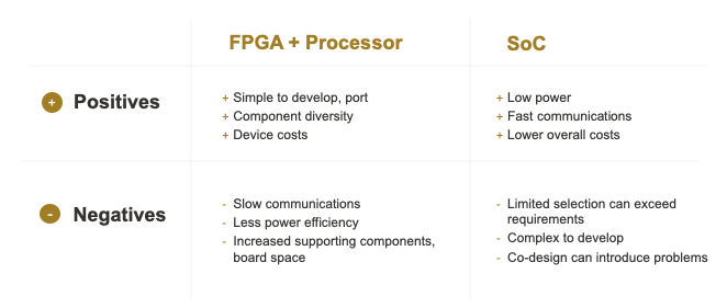
Choosing an FPGA + Processor setup offers a high degree of flexibility and simplicity. Decoupled development enables independent testing and easier porting of existing designs. The wide range of available processors and peripherals maximizes the ability to accommodate diverse project needs. For example, selecting from various ARM Cortex-M or RISC-V processors with different integrated peripherals, can tailor the system to specific requirements.
In contrast, SoCs add substantial performance benefits but also raise the level of design complexity. The co-dependent nature of PS and PL designs necessitates co-design, which can be a steep learning curve for designers unfamiliar with SoCs. The added complexity serves to enable sophisticated solutions, such as using EMIO and PL IP Cores to manage numerous PS-controlled UART hosts efficiently. Many vendors offer graphical PL block design tools to instantiate and connect vendor-provided IP Cores. It can be challenging to integrate custom RTL code into these tools in a way that couples performance with tight software control.
Many SoCs allow PS and PL to share access to On-Chip Memory (OCM) and external memory resources (like DDR). While this shared memory architecture is powerful, improper design can result in unexpected performance bottlenecks. It’s crucial to design memory access patterns that are carefully crafted to avoid contention, thereby minimizing latency and maximizing throughput.
Initial component costs for an FPGA + Processor setup may be lower, but an SoC can reduce the need for additional components, including clocks, power converters, volatile memory, and nonvolatile memory. For instance, the PL in an SoC can use a clock generated by the PS, and the unified power scheme simplifies power management. These reductions can lead to significant PCB cost savings due to less physical board space and fewer external signals.
While development costs for FPGA + Processor implementations might be lower due to simpler designs and readily available expertise, achieving optimal performance without the integrated features of an SoC can be challenging. The complexity of optimizing separate components for peak performance can offset initial cost savings.
In those cases where you have chosen an FPGA + Processor implementation, deploying an SoC for Hardware In Loop (HIL) testing can accelerate development and verification. Consider a design where an FPGA reads samples from an ADC, executes DSP algorithms, and outputs to a DAC, while a Processor manages the coefficients and monitoring. HIL testing with an SoC, where the PS can inspect and inject ADC samples and DSP results along the processing pipeline in real time, enables early validation of FPGA blocks. Consider using an SoC development board with PL fabric from the same family as the FPGA (e.g., UltraScale+) and I/O breakouts supporting required standards. HIL testing enables designers to isolate and verify many FPGA blocks efficiently before production boards are available. This approach helps to ensure robustness and reliability, reducing the risk of functional failures and warranty returns.
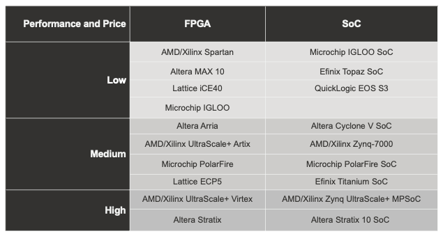
Choosing the right family of FPGA or SoC is crucial as it affects performance and price points. Key factors include clocking capabilities (maximum speed and number of PLLs), I/O capabilities (speed and flexibility), logic density, and the quantity and capability of hard blocks (e.g., BRAM, DSP Multipliers, MGT Interfaces). For SoCs, the quantity and the capabilities of the PS processors and integrated peripherals are also important.
For example, an UltraScale+ SoC might offer high-performance PS with multiple ARM Cortex-A53 cores and advanced PL capabilities, while a lower-end Zynq-7000 SoC might provide sufficient performance for less demanding applications. Selecting the appropriate family that aligns with your project’s requirements ensures a balance between performance and cost.
The table below provides illustrative examples of devices at different price/performance levels: