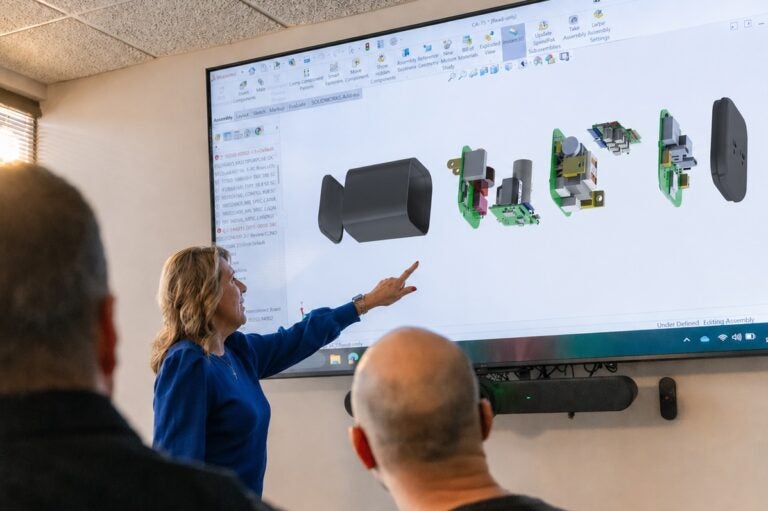
With over 1,000 successful projects involving custom PCBs under our belt, we have the experience in analysis, design, and layout to handle the most complex designs. Our team of IPC-certified designers, with an average of over 30 years of experience, utilizes cutting-edge Altium Designer CAE tools to deliver hand-routed PCBs that meet the highest industry standards. We collaborate closely with our customers throughout the design process, from requirements gathering and schematic capture to PCB/CCA design and procurement. Our team can support your procurement efforts or handle the entire process using our approved supplier network for complete PCB and PCBA prototyping and bring-up.
Re:Build AppliedLogix excels in a wide range of advanced PCB layout techniques, including high-speed signal integrity, power integrity, and advanced routing methodologies. Our expertise spans various domains, including high-frequency designs, high-power applications, and complex memory subsystems. We leverage cutting-edge tools and methodologies to deliver reliable, high-performance PCBs tailored to your needs.
Re:Build AppliedLogix has an impressive track record with over 1,000 successful PCB layouts delivered. Our team of highly skilled IPC-certified designers have decades of combined experience in tackling intricate design challenges. This wealth of knowledge ensures that your project receives the attention and expertise it deserves.
As an electronics design company, we leverage industry-leading tools like Altium Designer and Mentor Hyperlynx to drive innovation and efficiency in every project. Our circuit board design services are meticulously refined, incorporating advanced techniques such as 100% hand-routing with customized constraints, rigorous DFM/DFT/DFA analysis, and comprehensive thermal and signal integrity simulations.
At AppliedLogix, we prioritize your unique needs and objectives. Our dedicated team collaborates closely with you throughout the entire design cycle, providing tailored solutions that address your specific requirements. Through our PCB design and consulting sersvices, we are committed to delivering high-performance, reliable PCBs that exceed your expectations while maintaining open communication and fostering a strong partnership.
PCB layout services typically require 1-6 weeks, depending on component count, board complexity, layer count, routing density, and signal integrity requirements.
Less complex PCB layouts with lower component counts, standard interfaces, and straightforward routing can often be completed within 1-2 weeks. More advanced designs involving high pin-count devices, dense routing, high-speed interfaces, RF circuitry, impedance-controlled routing, or complex stackups generally require 4-6+ weeks to ensure proper design validation and optimization.
Project timelines may also be influenced by schematic completeness, design reviews, simulation requirements, and customer-specific documentation or manufacturing deliverables. Re:Build AppliedLogix works closely with customers throughout the process to establish realistic schedules while maintaining quality, manufacturability, and performance objectives.
Re:Build AppliedLogix follows industry-standard PCB layout practices based on the IPC-2220 family of standards while incorporating customer-specific requirements, manufacturer capabilities, and application-specific design constraints.
Our PCB layout process incorporates Design for Manufacturability (DFM), Design for Assembly (DFA), and Design for Testability (DFT) principles to help ensure designs can be fabricated, assembled, and tested efficiently. Design rules are tailored to each project and may include trace width and spacing requirements, impedance-controlled routing, creepage and clearance requirements, via and annular ring constraints, component placement guidelines, and manufacturer-specific fabrication limits.
For high-speed, high-power, or high-voltage designs, we also implement specialized design rules related to signal integrity, power integrity, thermal performance, and electrical safety. This approach helps ensure each PCB layout is optimized for performance, reliability, and manufacturability.
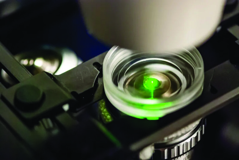
Yes. Re:Build AppliedLogix provides PCB layout services for RF and microwave circuits ranging from DC to 10+ GHz including Wi-Fi, Bluetooth, cellular, GPS, and custom wireless applications. We apply techniques such as coplanar waveguide and microstrip 50Ω transmission line routing, continuous ground planes, via stitching for shielding, proper matching networks, and strategic antenna placement. We also leverage electromagnetic simulation tools and signal integrity analysis tools to help ensure reliable high-frequency performance, minimize signal loss, and reduce EMI-related issues.
Re:Build AppliedLogix uses Altium Designer as its primary platform for for schematic, capture, PCB layout, design review, and documentation. Standardizing on a common design environment improves collaboration, consistency, and quality across our team of IPC-certified designers.
For advanced simulation and analysis, we use industry-leading simulation tools including HyperLynx, Simbeor, and Keysight ADS to evaluate signal integrity, power integrity, and RF behavior. These tools help identify potential issues before fabrication and support informed design decisions through the development process.
By combining PCB layout expertise with advanced simulation and verification capabilities, Re:Build AppliedLogix helps customers reduce design risk, improve first-pass success, and accelerate product development.
Re:Build AppliedLogix handles thermal management in PCB Layout through a combination of thermal analysis, strategic component placement, and optimized board design techniques. Our approach includes maximizing copper area for effective heat spreading, implementing thermal vias to transfer heat, selecting appropriate copper weights, and arranging components to support proper airflow and minimize thermal hotspots. For high-power or thermally sensitive designs, we use thermal simulation tools to verify operating temperatures remain within component specifications.
Design for Manufacturing (DFM) is the practice of designing a PCB so it can be fabricated, assembled, and tested reliably and cost-effectively. Effective DFM reduces manufacturing risk by ensuring the design aligns with the capabilities and limitations of the selected PCB fabricator and assembly partner.
Re:Build AppliedLogix incorporates DFM principles throughout the PCB layout process by reviewing trace widths and spacing, annular rings, drill sizes, solder mask clearances, component placement, assembly accessibility, and test point coverage. We also coordinate with fabrication and assembly partners when necessary to validate design rules and manufacturing requirements before release.
Strong DFM practices help reduce manufacturing defects, minimize prototype re-spins, improve production yield, shorten time to market, and lower overall product costs.
Re:Build AppliedLogix minimizes EMI/EMC issues through proven PCB layout practices designed to improve signal and power integrity and help products pass compliance testing with fewer design iterations and reduced chamber retesting. Our approach includes continuous ground planes providing low-impedance return paths, minimizing loop areas, proper decoupling within 5-10mm of power pins, filtering I/O connections, separating noisy digital and sensitive analog sections, avoiding routing over plane gaps, and using differential signaling for high-speed clocks. We also consider stackup design, shielding, and return current paths early in the layout process to reduce radiated and conducted emissions while improving overall system reliability.
Fill out the form below and someone from the Re:Build AppliedLogix team will be in touch with you shortly.